Les circuits intégrés GaN améliorent le rendement d'alimentation
Avec la contribution de Rédacteurs nord-américains de DigiKey
2025-10-28
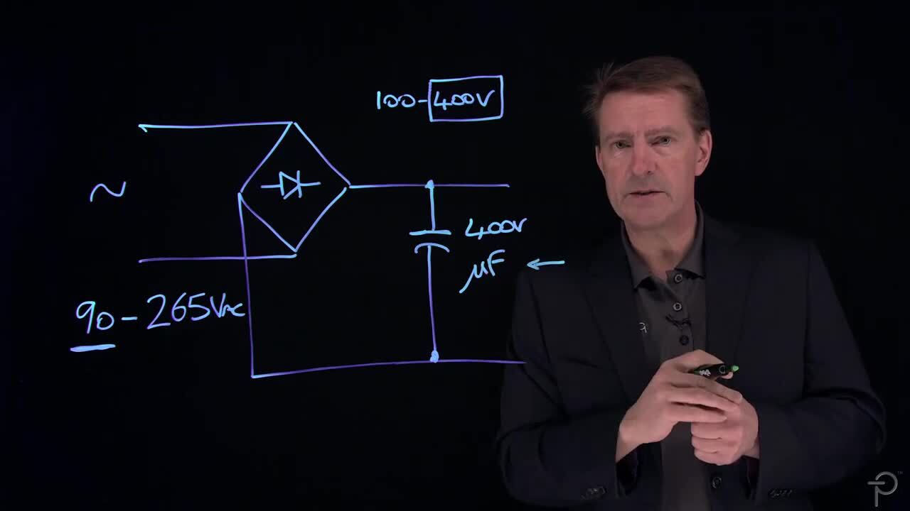
Dans le monde électronique actuel, les convertisseurs de puissance sont indispensables pour tous les types d'applications, des dispositifs médicaux aux chargeurs de téléphones et d'ordinateurs portables en passant par les alimentations auxiliaires. La miniaturisation des boîtiers, la gestion de la chaleur, les tensions d'entrée variables et les protocoles de charge intelligents sont autant de facteurs qui compliquent la conception des alimentations et des convertisseurs, tandis que dans le même temps, le rendement est de plus en plus important.
Au cours des dix dernières années, de nouvelles technologies de commutation ont émergé utilisant des circuits intégrés sur des puces en nitrure de gallium (GaN). Les circuits GaN présentent un comportement différent à l'échelle atomique, ce qui constitue à la fois des défis et des solutions pour les concepteurs de convertisseurs de puissance.
Les semi-conducteurs GaN ont une large bande interdite ; à 3,4 eV, elle est plus de trois fois supérieure à celle des semi-conducteurs en silicium. Comme d'autres matériaux à large bande interdite, les semi-conducteurs GaN sont capables de fonctionner à des tensions plus élevées, à des températures jusqu'à +400°C permettant leur utilisation dans des applications à plus haute puissance, et à des fréquences plus élevées les rendant utiles dans les applications radiofréquences (RF) et 5G.
Dans les applications de convertisseurs de puissance, les circuits intégrés GaN optimisent les pertes liées aux transistors telles que l'impédance série (RDS(ON)) et la capacité parallèle (COSS) avec des dimensions physiques inférieures à celles des circuits intégrés silicium. À empreinte égale avec un circuit intégré silicium, les circuits intégrés GaN peuvent gérer des fréquences plus élevées tout en générant moins de chaleur, une propriété permettant aux concepteurs de réduire voire d'éliminer les dissipateurs thermiques encombrants.
Cependant, les transistors GaN peuvent être difficiles à contrôler. Leur tolérance aux hautes fréquences signifie que le circuit d'attaque de commande doit être physiquement proche du transistor pour éliminer la latence et ralentir efficacement la vitesse de commutation du transistor, évitant ainsi les interférences électromagnétiques (EMI) indésirables. Les concepteurs de convertisseurs de puissance qui utilisent le GaN surmontent ces défis en utilisant un seul dispositif qui combine des commutateurs de puissance haute tension pour le côté primaire (entrée) et des circuits intégrés de commande pour le côté secondaire (sortie), ainsi que des circuits de rétroaction.
Spécificités de commutation
Power Integrations a créé plusieurs gammes de ces boîtiers utilisant sa technologie InnoSwitch3 avec PowiGaN™. Par exemple, la gamme de circuits intégrés d'alimentation à découpage InnoSwitch3-CP (Figure 1) utilise des contrôleurs indirects (flyback) quasi-résonants (QR) pour fournir des sorties à tension constante (CV)/courant constant (CC) pour un profil de puissance constante (CP).
Les côtés primaire et secondaire du circuit intégré sont isolés galvaniquement, mais les informations de tension et de courant de sortie sont transmises du contrôleur secondaire au contrôleur primaire via un couplage inductif. Cette technologie de communication FluxLink fournit rapidement des informations précises pour permettre des réponses transitoires de charge rapides et des fréquences de commutation jusqu'à 70 kHz.
 Figure 1 : La gamme de circuits intégrés d'alimentation à découpage InnoSwitch3-CP comprend des contrôleurs primaires et secondaires isolés galvaniquement, mais partageant une rétroaction via une liaison magnétique (ligne pointillée). (Source de l'image : Power Innovations)
Les circuits intégrés de la gamme InnoSwitch3-CP peuvent supporter de 50 W à 100 W sans dissipateurs thermiques, réduisant ainsi le volume global de l'alimentation. Ces composants sont répertoriés pour un fonctionnement continu à 650 V, mais peuvent résister à des surtensions jusqu'à 750 V. Les modèles industriels sont conçus pour supporter 900 V ou 1700 V.
Les alimentations utilisant des circuits intégrés de la gamme InnoSwitch3-CP démontrent un rendement de 94 % sur la plage de charge admissible, contre environ 90 % pour les commutateurs silicium. Ce haut rendement, associé à une consommation d'énergie minimale (moins de 30 mW), permet à la gamme InnoSwitch3-CP de respecter les réglementations mondiales en matière de rendement énergétique.
Pour garantir la sécurité et la longue durée de vie des composants, la gamme de circuits intégrés InnoSwitch3-CP est dotée d'une isolation galvanique renforcée de 4000 VCA conformément à la norme Underwriters Laboratories (UL) 1577 entre les côtés primaire et secondaire, et chaque unité fait l'objet d'un test diélectrique. Les autres fonctions de sécurité incluent la détection et la réponse à une grille ouverte dans le transistor à effet de champ du redresseur synchrone (SR FET), la protection contre la sous-tension ou la surtension de ligne d'entrée, et la protection contre la surtension de sortie. Le contrôleur de circuit intégré peut également limiter la surintensité et s'arrêter avant la surchauffe.
Les circuits intégrés de la gamme InnoSwitch3-EP (Figure 2) sont similaires à ceux de la gamme InnoSwitch3-CP. Au lieu d'être optimisés pour une seule sortie à puissance constante, ils utilisent une régulation côté secondaire (SSR) pondérée pour faire la moyenne des tensions de plusieurs sorties dans un signal de commande.
 Figure 2 : Les circuits intégrés d'alimentation à découpage InnoSwitch3-EP offrent une plage de puissance de sortie dépendant de la tension d'entrée. Schématiquement similaires aux circuits intégrés InnoSwitch3-CP, ils présentent une résistance de détection du courant optionnelle côté secondaire. (Source de l'image : Power Innovations)
Les circuits intégrés InnoSwitch3-EP sont également dotés d'une sortie dépendante de la tension. À 750 V, les circuits intégrés InnoSwitch3-EP produisent de 50 W à 100 W, et à 1250 V, ils produisent jusqu'à 85 W. Conçus pour un fonctionnement de commutateur haute tension, ils ont une tension de claquage de 1700 V.
Côté secondaire, une résistance de détection du courant est disponible en option pour la gamme InnoSwitch3-EP. Lorsque cette capacité de détection est activée, les unités peuvent être configurées pour redémarrer automatiquement si le courant de charge est supérieur à un seuil défini pendant une durée prédéterminée.
Les circuits intégrés InnoSwitch3-CP sont souvent choisis pour les convertisseurs de puissance grand public tels que ceux conçus pour le protocole USB Power Delivery (PD), le protocole QuickCharge (QC) ou d'autres protocoles propriétaires. Grâce à leur tenue en tension plus élevée et à leur flexibilité, les circuits intégrés InnoSwitch3-EP constituent un bon choix pour les alimentations en environnements industriels, et pour les compteurs d'énergie et les réseaux électriques intelligents. Ils sont également utilisés dans les alimentations auxiliaires, de secours et de polarisation des appareils électroménagers.
Alimentation programmable
Une gestion plus dynamique des entrées, des sorties et des défaillances est disponible avec les circuits intégrés InnoSwitch3-Pro (Figure 3) via une interface numérique I2C. Les utilisateurs peuvent également définir la fréquence de commutation à pleine charge sur une valeur personnalisée entre 25 kHz et 95 kHz, en choisissant une valeur plus basse pour minimiser l'accumulation de chaleur dans les grands transformateurs ou des fréquences plus élevées pour les petits transformateurs.
 Figure 3 : La gamme de circuits intégrés d'alimentation à découpage InnoSwitch3-Pro est configurée pour être contrôlée numériquement via une interface I2C permettant la surveillance à distance de l'état, le réglage de la tension et du courant, et une fréquence de commutation personnalisée. (Source de l'image : Power Innovations)
La présence d'un microcontrôleur dans la boucle offre aux circuits intégrés InnoSwitch3-Pro des options de protection supplémentaires. Les utilisateurs peuvent configurer de manière indépendante les réponses souhaitées aux défauts de surtension et de sous-tension de sortie. Ils peuvent également surveiller la tension d'entrée et garantir la protection contre les situations de baisse de tension/hausse de tension et les surtensions. Le microcontrôleur détecte également les grilles SR FET ouvertes et gère le blocage thermique hystérétique pour mieux protéger le circuit intégré.
Grâce à leur conception hautement configurable, leur faible dissipation thermique et leur haut rendement, les circuits intégrés InnoSwitch3-Pro conviennent parfaitement à une utilisation dans les adaptateurs de charge conformes à des protocoles comme USB PD 3.0, QC, AFC (Adaptive Fast Charge), FCP (Fast Charge Protocol) et SCP (Super Charge Protocol). Les concepteurs les choisissent également pour les chargeurs de batterie et les ballasts LED réglables où des conceptions compactes avec une accumulation de chaleur minimale sont requises.
Condensateurs compacts
Les circuits intégrés de commutation tels que ceux de la ligne InnoSwitch3 ne représentent qu'une petite partie de l'architecture des alimentations et des convertisseurs de puissance. Par exemple, un condensateur de masse, qui est un composant de stockage d'énergie lissant les fluctuations de courant alternatif entrant dans une alimentation, peut occuper jusqu'à 25 % de l'espace dans cette alimentation.
En utilisant la technologie de commutation PowiGaN, Power Integrations a développé MinE-CAP, un commutateur et contrôleur fonctionnant avec deux condensateurs plus petits pour fournir la capacité appropriée pour une tension d'alimentation donnée (Figure 4). Un condensateur céramique ou électrolytique pouvant supporter jusqu'à 400 V et répertorié de 1 µF à 5 µF est toujours actif. MinE-CAP active un condensateur électrolytique supplémentaire répertorié pour 160 V mais avec une capacité plus élevée lorsqu'une tension inférieure est détectée.
En plus de réduire l'espace nécessaire jusqu'à 40 % en divisant le condensateur de masse en deux moitiés plus petites, MinE-CAP élimine également le recours à une thermistance à coefficient de température négatif (CTN) d'appel. Les condensateurs contrôlés par MinE-CAP sont dimensionnés pour gérer le courant d'appel à la mise sous tension de l'alimentation.
 Figure 4 : MinE-CAP est un contrôleur de circuit intégré basé GaN qui permet de diviser le condensateur de masse d'une alimentation en deux unités plus petites, réduisant ainsi le volume nécessaire jusqu'à 40 %. MinE-CAP est conçu pour fonctionner avec les produits de conversion CC/CC InnoSwitch3. (Source de l'image : Power Innovations)
Conclusion
Les circuits intégrés de commutation qui combinent des transistors, des circuits intégrés de commande et des circuits de rétroaction utilisant des semi-conducteurs GaN tirent parti de la résistance aux hautes températures, tensions et fréquences de ce matériau. Ces circuits intégrés permettent de réduire la taille des circuits imprimés, d'éliminer les dissipateurs thermiques et d'optimiser le placement des condensateurs, de sorte que les alimentations multifonctions peuvent être intégrées dans des boîtiers plus compacts. Les produits GaN tels que les lignes InnoSwitch3 avec PowiGaN de Power Integrations vont sans aucun doute continuer à intéresser les concepteurs en quête d'une plus haute densité de puissance et d'une miniaturisation accrue.
Avertissement : les opinions, convictions et points de vue exprimés par les divers auteurs et/ou participants au forum sur ce site Web ne reflètent pas nécessairement ceux de DigiKey ni les politiques officielles de la société.